Photo Etching division
- HOME
- Photo Etching division
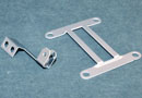
We conduct precision work on metallic materials using photo etching technology, supplying products to a wide variety of industries including electronic components.
The process of photo etching utilizes the corrosive effects of metals, enabling precision work at the micrometer level without causing burrs.
Compared with press and laser work, photo etching work costs less, can be ordered in small lots, and can be delivered faster at lower prices.
We can integrate everything from design to completion, so please tell us your needs.
Applications
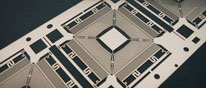
Lead Frame
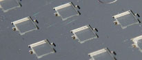
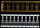
Carrier tray

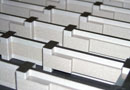
Shim, Spacer
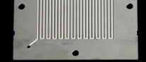
Microreactor
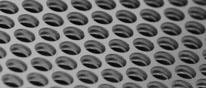
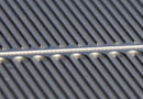
Mesh, Filter
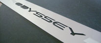
Exterior parts
Processing technology
Single face etching
We can make designs that are thin on the whole, and grooves on the front and back sides of thick areas. (Useful for fuel cells, heat exchangers, microreactor, etc.)
Surface treatment
We handle a variety of surface treatments such as Au, Ag, Ni, Cr, Cu etc. plate processing, electropolishing and chemical polishing.
Lamination process
Grafting together etching-processed components through diffusion bonding/spot welding allows us to achieve layered states impossible to attain with mechanical processing, such as the creation of irregularly shaped layer stacks and cavity layers.
Etching +α
We offer processed products that meet customer needs by combining processes such as bending, stamping, electrical discharge machining and laser finishing.