Detailed specification
- HOME
- Circuit board division
- Detailed specification
We manufacture various circuit boards using screen printing (thick films) and PVD (thin films) technologies with photolitho technology.
Our products are being supplied to a wide variety of fields, such as communications devices and industrial instruments including satellites and base stations, sensors, consumer devices and displays.
We provide highly dependable precision circuit boards for whatever our customers' needs may be, so please feel free to inquire.
Detailed specification
Thick film technology
- Substrate
- Ceramic, Glass, PI, PEN, PET, Metallic board etc
- Paste
- Glass, Ag, Au, Pt, Pi, Solder resist, Carbon etc
- Film thickness
- 0.2μm〜100μm
- Line width
- Line / Space ≧ 100 / 120μm
- Processing size
- less than 1000x1600mm
Thin film technology
- Substrate
- Ceramic, Glass, AIN etc
- Sputtering
- Cr, Ti, Pd, Cu, Au, NiCr, TaN
- Deposition
- Cr, Ti, Pd, Ni, Mo, Au, Pt
- Plating
- Au, Ag, Cu, Ni, Sn etc
- Film thickness
- Total thickness 2〜5μm
- Line width
- Line / Space ≧ 30μm *Au2.0μm
- Processing size
- less than 100x100mm
Design rule of thin film formation of substrate processing
| Substrate thickness | 0.1 | 0.25 | 0.38 | 0.635 | 1 | |
|---|---|---|---|---|---|---|
| # | Corresponding point | min. dimension | min. dimension | min. dimension | min. dimension | min. dimension |
| A | Externai form (dicing) | 0.5 | 0.5 | 0.5 | 0.8 | 2 |
| B | External form (interval of dicing point to laser point) | 1 | 1 | 1 | 2 | 2 |
| C | External form (Interval of laser point to laser point) | 0.25 | 0.25 | 0.4 | 0.4 | 0.8 |
| D | Between a substrate edge and a hole | 0.5 | 0.5 | 0.5 | 0.5 | 0.8 |
| E | A through hole | 0.12 | 0.2 | 0.2 | 0.3 | 0.4 |
| F | Between a through-hole and a pattern | 0.1 | 0.1 | 0.1 | 0.1 | 0.1 |
| G | Between a pattern and a hole | 0.1 | 0.1 | 0.1 | 0.1 | 0.1 |
| H | Between a substrate edge and a pattern | 0.05 | 0.05 | 0.05 | 0.05 | 0.05 |
| R | Corner R with laser | 0.1 | 0.1 | 0.1 | 0.2 | 0.2 |
(mm)
Design rule of thin film formation of the parttern
| Plating material used as a conductor | Au, Sn | Cu / Ni / Au (Pd-Free) | |||||
|---|---|---|---|---|---|---|---|
| Thickness | 2μm | 5μm | 3μm/ 1μm/ 1μm | ||||
| # | Corresponding point | min. dimension | Tolerance | min. dimension | Tolerance | min. dimension | Tolerance |
| W | Width of a conductor | 0.03 | ±0.01 | 0.04 | ±0.01 | 0.05 | ±0.01 |
| I | Width of a resistance | 0.1 | ±0.01 | 0.1 | ±0.01 | 0.1 | ±0.01 |
| J | Length of a resistance | 0.1 | ±0.01 | 0.1 | ±0.01 | 0.1 | ±0.01 |
| S | Between patterns | 0.03 | ±0.01 | 0.04 | ±0.01 | 0.05 | ±0.01 |
(mm)

*Tolerance of dicing processing; ±0.05 mm
*Tolerance of laser processing; ±0.1
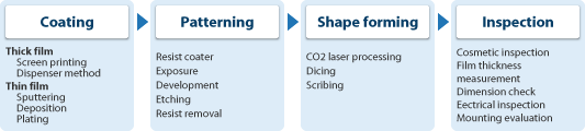
Process flow
Inspection
We conduct evalution and decision with various measuring devices to meet the required quality standards.
- Film thickness
- X-ray fluorescence thickness meter, Surface profiler
- Pattern width
- Profile projector, Metallurgical microscope
- External form of substrate、Substrate thickness
- Digital calipe, Digital micrometer
- Sheet resistance
- Four-terminal sensing (4T) method
Reliability test
We have a lot of devices for environmental test and analysis to check and enhance the quality of product.
- High temperature chamber, Low temperature chamber, Thermal shock chamber, Humidity chamber
- TCR (temperature coefficient of resistance), Migration, Solder wettability, Tensile strength, etc...
- Microscopes; Optical microscope, Laser Microscope etc
Combination technologies
- CO2 laser processing ...... Shape forming, Through-hole making
- Sandblast or microblasting processing ...... Shape forming, Through-hole making
- Dicing processing
- Glass scribing, Laser scribing
- Plasma spray coating
- Polishing processing